I've recently completed a small circuit-prototyping project and would like to pass along some of what I've done to others.
Over the years I've done a number of small RF and analog circuit designs, using several variants of what's known as "ugly" or "Manhattan" construction. These involve building a circuit (using primarily leaded or "through-hole" components) directly on a piece of PC-board stock, without first laying out and etching specific board traces for the individual circuit.
There's a very nice overview of some of these sorts of techniques at Clifton Laboratories and more at this page
The latter link shows a picture of Ivanboard, a commercial product available some years ago which had a premade set of square "island" pads. I saw this listed for sale years ago (in Audio Amateur, I think) but as far as I can tell it's off the market these days... and it wasn't cheap.
After doing a small project recently using the "core drill" technique, I decided there had to be a better way. Making an array of circular pads with a core drill was a bit laborious, generated a lot of nasty dust from the FR4 board substrate, and it wasn't easy to get a completely regular pattern. I also had to drill through the board and solder in wires to tie the upper part of the ground plane to the full-fill ground on the bottom of the board.
So, I sat down with KiCAD, made up a minimal board (just one or two pads), looked through the resulting board-description file, and wrote a Perl "array of pads" generator script to create suitable boards automatically. The script lays down the pads, "drills" vias, ties the vias and grounds together with copper traces, and adds ground-fill zones on both sides. I import the resulting board file into KiCAD, tell KiCAD to fill the zones, and then generate Gerber photoplot files ready for manufacture.
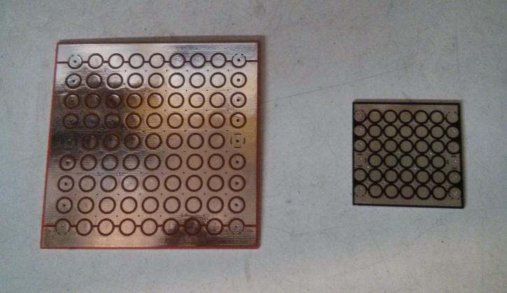
I've done two such boards now:
a 6x7 array of small pads which fits
in a 5 cm square
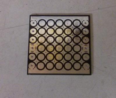
and a 9x9 array which fits in a 10 cm square.
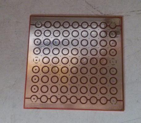
The pads along the left and right sides are drilled for wire attachments, and there are "power rails" along the upper and lower edges of the boards to allow for single- or dual-polarity power supplies. The bottom is a solid ground plane, covered with solder mask. The top has ground-plane fill between the pads, with each patch being stitched to the bottom with a via, and is un-masked except for around the isolation "rings". Surface-mount components can be bridged from a pad to the ground fill, or (on the smaller board) between adjacent pads (use the 1206 size for this).
By no coincidence at all, the two board sizes are ones that can be made quite inexpensively by DirtyPCBs.com via their "proto pack" offer (10 boards, plus or minus one or two, with solder mask and HASL surface "tinning", for a low fixed price). I just got my first order back (about a month after I uploaded the Gerbers) and I'm quite satisfied with the quality.
Since these boards might be useful to other experimenters, I've added them to the DirtyPCBs.com store - you can order 'em from these folks at their current "proto pack" price (disclaimer: I would get a small credit or payment from them for each order). Or, if you would prefer to have some made at a different board house, or would like to etch a few yourself, you can download the Gerber files:
I'm releasing these Gerbers under a Creative Commons license, so you're free to use 'em as long as you give credit.
Happy prototyping!
Dave Platt AE6EO (dplatt@radagast.org)